S
R
Q(t+1)
| S |
R |
Q(t) |
Q(t+1) |
|---|---|---|---|
| 0 | 0 | 0 | 0 |
| 0 | 0 | 1 | 1 |
| 0 | 1 | 0 | 0 |
| 0 | 1 | 1 | 0 |
| 1 | 0 | 0 | 1 |
| 1 | 0 | 1 | 1 |
| 1 | 1 | 0 | undefined |
| 1 | 1 | 1 | undefined |
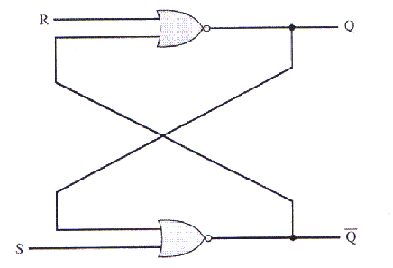
To understand how the flip-flop works, here is an explanation of the defined cases:
- R = S = 0 and Q = 0 (no change):
- The inputs to the lower NOR gate are S = 0, Q = 0, so the output Q = 1. This output is fed to the upper NOR gate, so its inputs are R = 0 Q = 1, so the output Q = 0.
- R = S = 0 and Q = 1 (no change):
- The inputs to the lower NOR gate are S = 0, Q = 1, so the output Q = 0. This output is fed to the upper NOR gate, so its inputs are R = 0 Q = 0, so the output Q = 1.
- R = 0 S = 1 and Q = 0 (set):
- The inputs to the lower NOR gate are S = 1, Q = 0, so the output Q = 0. This output is fed to the upper NOR gate, so its inputs are R = 0 Q = 0, so the output Q = 1.
- R = 0 S = 1 and Q = 1 (set):
- The inputs to the lower NOR gate are S = 1, Q = 1, so the output Q = 0. This output is fed to the upper NOR gate, so its inputs are R = 0 Q = 0, so the output Q = 1.
- R = 1 S = 0 and Q = 0 (reset):
- The inputs to the lower NOR gate are S = 0, Q = 0, so the output Q = 1. This output is fed to the upper NOR gate, so its inputs are R = 1 Q = 1, so the output Q = 0.
- R = 0 S = 1 and Q = 1 (reset):
- The inputs to the lower NOR gate are S = 0, Q = 1, so the output Q = 0. This output is fed to the upper NOR gate, so its inputs are R = 1 Q = 0, so the output Q = 0.
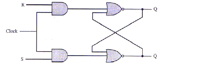
Here is the logic diagram for the SR flip-flop, which shows the inputs and outputs of the flip-flop. C is the clock input.
The problem with this device is that the output is undefined when S = R = 1.
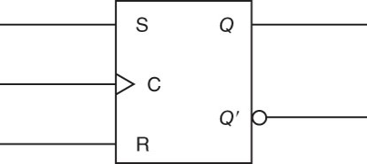
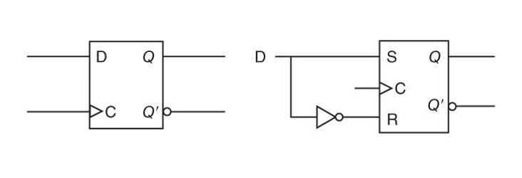
D Flip-Flop
The D flip-flop solves the problem of the undefined case in the SR flip-flop by elminating that case. Here is a clocked D flip-flop.
The D flip-flop is used to create a bit of memory. It is used in RAM and registers.
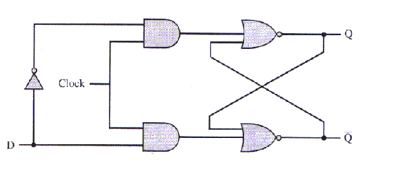
Here is the logic diagram for the D flip-flop, which shows the inputs and outputs of the flip-flop. C is the clock input.
Registers
A register stores a value in the CPU. The CPU contains control registers, general purpose registers, and floating point registers. These registers are the same type of circuit but they are used in different ways. Here is a logic diagram and a block diagram for a 4-bit register implemented with D flip-flops.
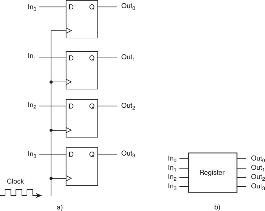
The register has 4 input lines, 4 output lines, and a clock signal. All bits in the register must accept a new input value and store it at the same time. The clock signal is tied into all 4 D flip-flops, so they all change value when the clock pulses.
The register also has lines for power, ground, and a clear line to allow the register to be reset to 0. For the sake of simplicity, these lines are not shown.
Counter
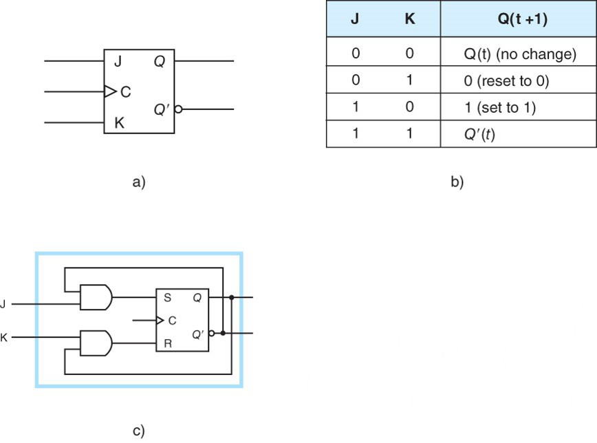
A counter is a circuit that adds 1 to its current value each time it is activated. The counter below uses JK flip-flops. JK flip-flops are like SR flip-flops, except that an input of 1 1 toggles the flip-flop. Here are the characteristic table and diagrams for the JK flip-flop.
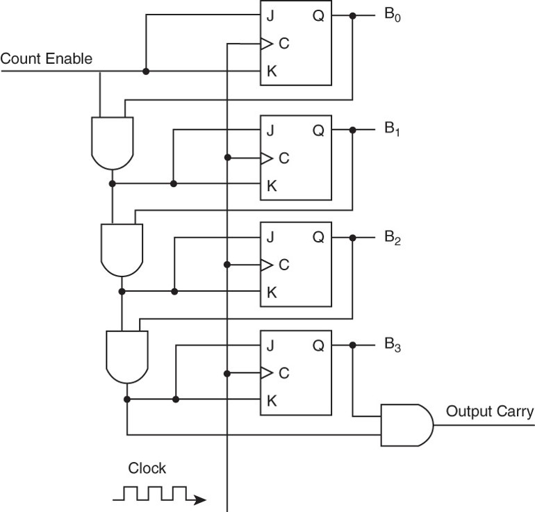
Here is the 4 bit counter. In the counter we see that the current state of each bit is used in updating the bit to its left. B0 flips every time the count enable is activated. When B0 changes from 1 to 0, B1 is activated and flips. This is when we "carry the 1" from B0 to B1. For the other bits, they change from 0 to 1 when all bits to the right are 1. You must trace through this circuit carefully to understand how it works, and make sure that it goes from 1111 back to 0000.
Email Me |
Office Hours |
My Home Page |
Department Home |
MCC Home Page
© Copyright Emmi Schatz 2016